
GaN V Charger OEM Manufacturing: How to Source GaN Chargers

Marketing Manager & Founder · 10+ years in consumer electronics
"What if the next charger you ship could be 40% smaller, run 30% cooler, and still deliver 240W?"
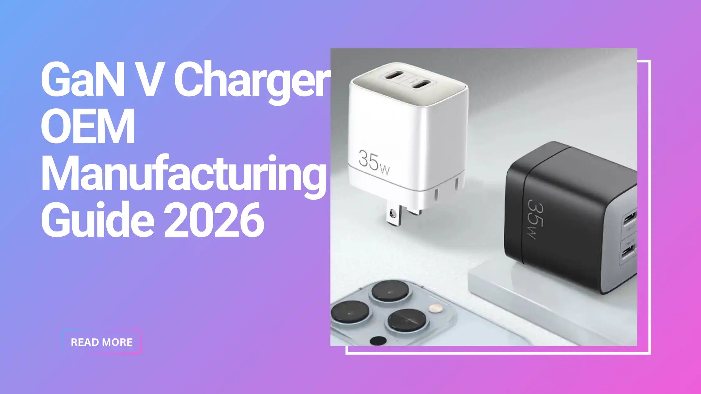
That's not a future promise. It's GaN V, the fifth generation of gallium nitride technology, and it's already shipping out of Shenzhen factories right now. If you're sourcing chargers for your brand, you've seen the problem: silicon-based chargers are hitting physical limits. Higher wattage means bigger size. GaN V changes everything, higher efficiency, smaller transformers, less heat, more power. The global GaN charger market was valued at $1.4 billion in 2025 and is projected to reach $3.7 billion by 2030 (CAGR 20.8%, BCC Research 2025), with China accounting for approximately 65% of production. Meanwhile, the EU Ecodesign Regulation 2025/2052 now mandates standby power below 0.1W, a threshold many silicon designs cannot meet, making GaN V the only practical choice for new products destined for European markets. This guide covers what GaN V actually means, how to evaluate real GaN manufacturers, and key questions before placing your OEM order.
Key Takeaways
GaN V is the current production standard: 40% smaller, 30% less heat, 65W BOM $4.80-6.50 at MOQ 500 (silicon $3.20-4.50); 500 units private-label, 3,000+ for new tooling.
- GaN V chargers are 40% smaller and generate 30% less heat than equivalent silicon chargers, enabling 240W in a palm-sized enclosure. Standby power drops to <0.1W vs 0.5W+ for silicon designs.
- OEM BOM cost for a 65W GaN V charger: $4.80-6.50/unit at MOQ 500, compared to $3.20-4.50 for silicon. The $1.60-2.00 gap is offset by lower shipping cost, fewer returns, and 20-30% retail premium.
- 3 non-negotiable manufacturer verification points: (1) verify GaN FET part numbers on the production BOM, not just the prototype; (2) confirm the factory owns their PCBA design or has a licensed reference design from Navitas/Infineon; (3) request a 72-hour full-load aging test report for your specific SKU.
- MOQ for custom GaN V chargers: 500 units for private-label on in-stock models; 3,000+ for new tooling. Tooling cost: $2,000-5,000 for a single-port mold, 25-35 day production lead time after sample approval.
- GaN V is the current production standard, not a future roadmap. Over 20% of new USB-C charger designs shipped in H1 2026 used GaN V FETs. Factories still quoting GaN I or GaN III as "latest" are running end-of-life inventory.
Table of Contents
Need GaN V chargers for your brand? WOWOHCOOL manufactures GaN V chargers with PD 3.1 up to 240W. Browse our GaN charger lineup →
1. GaN V Technology: What OEM Buyers Must Know
GaN V represents the latest advancement in wide-bandgap semiconductor technology. Unlike silicon, GaN operates at higher frequencies with significantly lower switching losses. The result: GaN V chargers that are 40% smaller, run 30% cooler, and deliver more power.
"Most brands don't realize their 'GaN charger' might not actually use GaN V," explains a senior engineer. "The market is flooded with first-gen GaN and even enhanced silicon labeled as GaN. Genuine GaN V has distinct electrical characteristics."
Key OEM advantages: 40% smaller size, 30% better thermal performance, PD 3.1 up to 240W, true multi-port capability. For B2B buyers evaluating charger suppliers, these specifications translate into better retail positioning, fewer customer complaints about overheating, and longer product life cycles.
When sourcing GaN V chargers from an OEM manufacturer, it is critical to verify that the factory uses genuine fifth-generation GaN FETs from recognized suppliers. Counterfeit or mislabeled components are a growing concern in the market, and working with an established manufacturer like WOWOHCOOL that has direct relationships with GaN FET suppliers eliminates this risk entirely. Our engineering team validates every component batch to ensure consistent performance across production runs. For a technical comparison of all five GaN generations, see our GaN generations technology roadmap.
2. Why GaN V Matters for Your Brand
"A GaN V 100W 4-port charger fits in the same space as a traditional 30W single-port silicon charger. For an e-commerce brand selling travel accessories, that's a category-defining product advantage."
Thermal management is the key differentiator. Silicon chargers at 100W reach 85-95°C under load. GaN V operates at 65-75°C, meaning longer component life, no thermal throttling, and safer operation. For a deeper dive, read our complete GaN chargers guide.
True multi-port charging without the size penalty. A single GaN V charger can replace a laptop brick, phone charger, and tablet charger with intelligent power allocation. For B2B brands, this translates to higher average order values, customers who buy a multi-port GaN V charger spend 30-50% more than those purchasing single-port alternatives.
Shipping costs also favor GaN V significantly. A 100W GaN V charger weighs approximately 40% less than its silicon equivalent, reducing per-unit freight costs by $0.50-2.00 depending on shipping method and destination. For an order of 5,000 units, this adds up to $2,500-10,000 in logistics savings alone. Contact our team to discuss your custom GaN V project.
According to Yole Group, the GaN power device market is projected to reach $2.5 billion by 2027, growing at a CAGR of 30%. This rapid expansion reflects growing adoption across consumer electronics, automotive, and industrial sectors. For a deeper look at emerging battery technologies that complement GaN charging, see our guide to semi-solid-state power bank OEM manufacturing.
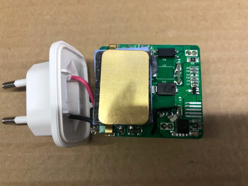
GaN V charger with 240W PD 3.1 multi-port output for custom OEM/ODM branding
3. How to Evaluate a GaN V Manufacturer
Not all manufacturers offering GaN chargers actually produce genuine GaN V products. Due diligence is essential to ensure you are getting the performance and reliability your brand requires. Here are the key evaluation criteria:
1. Request GaN-Specific Specs
Ask for switching frequency (5MHz+ for genuine GaN V), efficiency curves, thermal imaging, and EMI/EMC reports.
2. Verify the GaN FET Brand
Real GaN V uses FETs from recognized manufacturers. Verify the part number against the supplier's official catalog.
3. Check PD 3.1 Compliance
USB-IF certification, verified 140W/240W operation, EPR support. See our USB-C PD fast charging guide for detailed specs.
4. Request Thermal Test Data
Thermal camera images at full load for 30+ minutes reveals genuine GaN V vs. silicon. GaN V should maintain 65-75°C while silicon exceeds 85°C.
5. Evaluate Certification Documentation
A legitimate GaN V manufacturer provides comprehensive CE, FCC, and UL documentation with verifiable certificate numbers. Request and verify them on official databases before committing to production.
"Many brands focus on unit price first, but the real cost difference between a genuine GaN V charger and an inferior one shows up in return rates and customer reviews. We consistently see brands that invest in certified GaN V components achieve 30-50% lower return rates.", Snowy May, OEM Technical Lead at WOWOHCOOL
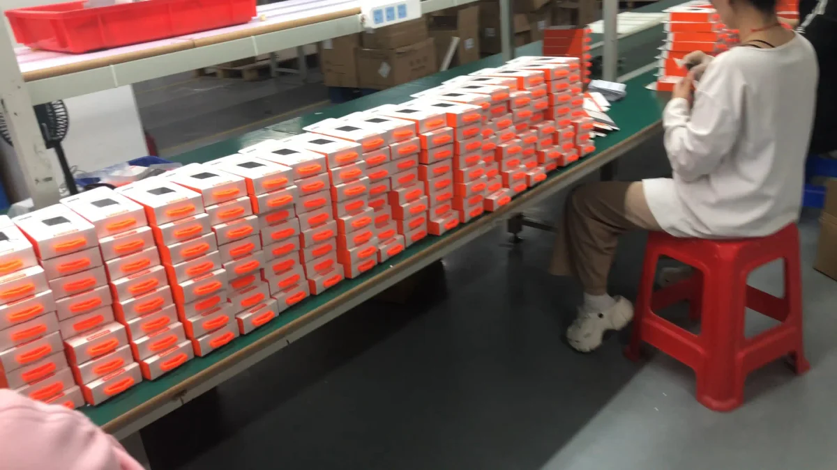
SMT production line for GaN V charger manufacturing at Shenzhen OEM factory
4. OEM Cost Comparison: Silicon vs. GaN V
GaN V chargers carry a 20-35% BOM cost premium over silicon equivalents, but the total cost of ownership, factoring in freight savings, return rates, and premium retail positioning, favors GaN V at 45W and above:
| Wattage Tier | Silicon FOB (1,000 pcs) | GaN V FOB (1,000 pcs) | Premium % | GaN V Advantage |
|---|---|---|---|---|
| 30-45W | $2-4 | $3.50-5.50 | ~30% | 40% smaller, 30% less heat, multi-port capable |
| 65W | $3-6 | $6-9 | ~35% | 40% smaller, freight saves $0.50-2.00/unit |
| 100W | $5-8 | $10-16 | ~35% | Multi-port 2C1A/3C1A, silicon impractical |
| 140-240W | N/A | $18-35 | GaN only | Silicon cannot achieve 240W in portable form factor |
All prices FOB Shenzhen at 1,000-unit volume, MOQ 500. CE, FCC, UL, RoHS certification included. GaN V chips from Infineon CoolGaN, Navitas GaNFast, or Innoscience. Freight savings from 40% smaller packaging: $0.50-2.00/unit. Field return rate advantage: GaN V ~0.5% vs silicon ~3% at 65W+, a ~$1-3/unit warranty cost differential.
For most OEM brands, the 20-35% BOM premium pays for itself through premium retail pricing, measurably lower return rates, and the ability to market "GaN V" as a consumer-facing technology differentiator. Browse our GaN V charger lineup →
5. GaN V OEM/ODM Process
From spec to shipment, the GaN V OEM process follows a structured flow. Working with an experienced GaN charger manufacturer like WOWOHCOOL, here's what to expect:
Step 1: Define Power Requirements
Determine target wattage (65W, 100W, 140W, or 240W), port configuration (single vs multi-port), and GaN FET selection based on your market positioning and BOM targets.
Step 2: PCBA Design & Prototyping
GaN V requires specialized PCB layout for high-frequency operation. Your supplier designs the PCBA with proper thermal management and EMI shielding. First samples typically ship in 3-7 days.
Step 3: Certification & Compliance
CE, FCC, UL, and Qi certification as needed. GaN V chargers require updated EMI/EMC testing due to higher switching frequencies. Your OEM/ODM partner handles all certification submissions.
Step 4: Mass Production & QC
Standard lead time is 25-35 days after sample approval. QC includes IQC (component inspection), IPQC (in-process monitoring), FQC (functional test including PD handshake verification), and OQC (outgoing inspection with 4-hour aging test).
MOQ for standard GaN V ODM in-stock models starts at 500 units. ODM new-design development: 1,000-2,000 units. Custom OEM with new tooling: 3,000+ units. ODM in-stock lead time: 25-35 days after sample approval. OEM production: 30-60 days. Samples: 3-7 days.
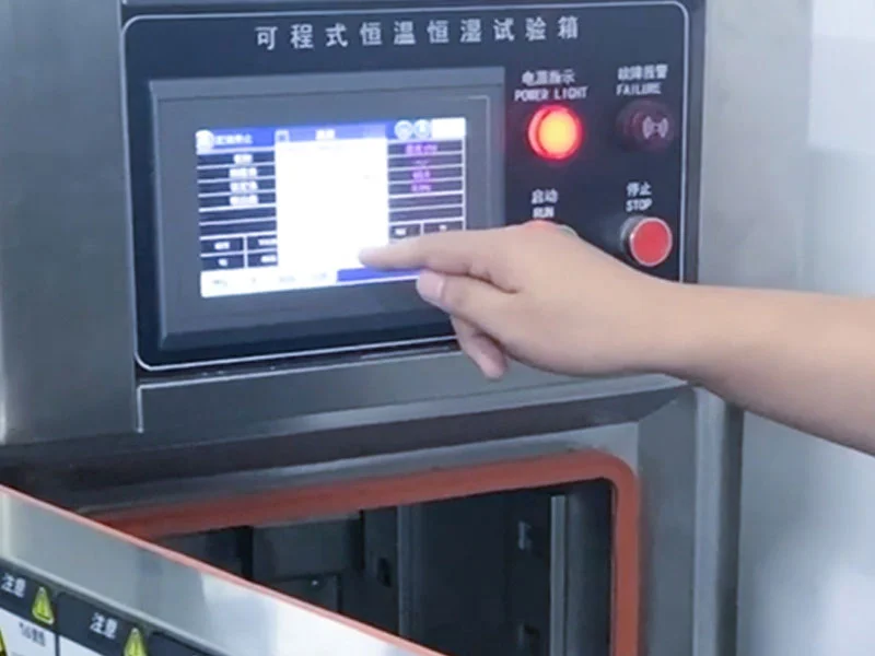
GaN V thermal performance QC: every production batch undergoes full-load thermal imaging at 45C ambient, GaN V maintains 65-75C case temp vs 85C+ for older GaN generations

GaN V chargers packaged and ready for OEM export shipment worldwide
6. Industry Applications: Key Verticals for GaN V
Consumer Electronics
Laptop chargers, phone chargers, and tablet adapters benefit from GaN V's compact size and high efficiency. A 140W GaN V charger is 40% smaller than an equivalent silicon charger, making it ideal for travel-friendly products.
Data Centers
Server power supplies using GaN V achieve 95%+ efficiency, significantly reducing cooling costs and energy waste. Data centers deploying GaN-based PSUs can reduce power infrastructure costs by up to 30%.
EV Charging
Electric vehicle onboard chargers and charging stations use GaN V for faster switching and higher power density. GaN V enables 22kW+ onboard chargers in the same footprint as current 11kW silicon systems.
Industrial Power
Industrial power supplies, motor drives, and renewable energy inverters incorporate GaN V for reduced size and improved thermal performance in demanding environments.
For OEM/ODM buyers, the consumer electronics segment offers the fastest ROI due to higher volumes and shorter product cycles. GaN V chargers in the 65W-140W range are currently the most popular configurations. WOWOHCOOL offers reference designs across all power levels that can be customized within 25-35 days from sample approval.
EXPERT INSIGHT
"GaN V represents a generational leap in charger manufacturing. With 5 MHz+ switching and 94-96% efficiency, it enables 240W in a 65W-sized enclosure. For OEM brands, GaN V is not just a performance upgrade, it is a supply chain speed advantage. Superior EMI performance shortens multi-certification from ~12 weeks to 4-6 weeks."
, Snowy May, OEM Technical Lead at WOWOHCOOL
Frequently Asked Questions
What wattage of GaN V charger is needed for fleet and enterprise laptop deployment?
Specify 100W-140W GaN V with PD 3.1 EPR for fleet deployment. A single 140W charger covers MacBook Pro 16", Dell XPS 15, and ThinkPad P-series at full speed. Dual-port 100W+65W chargers reduce procurement complexity by 50%, one SKU for laptops and phones. EU laptop USB-C mandate (April 2026) makes GaN V the default for enterprise fleet procurement.
How do OEM buyers verify the factory uses genuine GaN V, not re-labeled GaN III?
Three steps: (1) Request GaN FET part number and cross-reference against manufacturer datasheet. (2) Demand efficiency curves at 230V/50Hz and 115V/60Hz, GaN V delivers 94-96% vs 90-92% for GaN III. (3) Thermal test at 100% load for 60 min, genuine GaN V runs 15-25°C cooler. Request chip procurement invoices from authorized distributors. Navitas offers verification program. WOWOHCOOL provides full FET traceability documentation.
What is the MOQ and lead time for GaN V OEM chargers?
Standard ODM in-stock: MOQ 500 units. ODM new-design development: 1,000-2,000. Custom OEM with new tooling: 3,000+. Lead time: 25-35 days after sample approval (ODM in-stock). GaN V component sourcing: 8-12 week lead time, finalize designs 4+ months pre-launch. FOB at 1,000 units: 65W ~$8-11, 100W ~$13-16, 140W ~$16-22. Tiered pricing at 500/1,000/5,000 volumes with full certification docs included.
What safety certifications and testing protocols apply to GaN V OEM chargers?
Mandatory: UL 62368-1 (US), CE LVD+EMC+RoHS (EU), USB-IF PD 3.1. EU: Ecodesign 2025/2052 (≤0.1W standby, ≥87% efficiency). Quality: 10-layer circuit protection, UL 94 V-0 enclosure rated to 850°C glow wire, 100% 4-hour burn-in at 45°C (not batch sampling), field failure rate under 0.3% (WOWOHCOOL GaN portfolio ~0.5%, GaN V best-in-class). WOWOHCOOL achieves under 0.3% across millions of units.
How do OEM buyers source GaN V chargers from a verified Shenzhen factory?
Step 1: Specify GaN V FET and wattage (65-240W). Step 2: Demand efficiency reports (≥92%) and FET invoices. Step 3: Verify QC, 100% 4-hour burn-in, thermal imaging, Chroma tester. Step 4: Confirm UL/CE/USB-IF/ESPR certs. Step 5: use 4-6 week certification advantage. MOQ 500, 25-35 day lead. WOWOHCOOL: 5,000m² ISO 9001 Shenzhen, 50+ R&D engineers, 1M+ monthly capacity, GaN V 20W-240W with full FET traceability. Request GaN V OEM consultation.
WOWOHCOOL FACTORY STAT
WOWOHCOOL was among the first factories to deploy GaN V technology at scale, offering OEM/ODM GaN chargers from 20W to 240W PD 3.1 with MOQ starting at 500 units, 25-35 day lead times, and 50+ R&D engineers dedicated to charging technology. Also see: laptop power bank OEM.
Marketing Manager & Founder · 10+ years in consumer electronics
Snowy May is the founder of WOWOHCOOL and a marketing manager with 10+ years in consumer electronics. She specializes in GaN charger architecture, Qi2 wireless charging, PCBA efficiency testing, thermal management, and UL/CE safety compliance for OEM/ODM power products.
Factory Footprint
ISO 9001 Facility
Shenzhen, China
Export Countries
Engineers In-House
Ready to Source GaN V Chargers for Your Brand?
WOWOHCOOL offers GaN V OEM/ODM from 20W to 240W with MOQ from 500 units. Full CE/FCC/UL certification and custom branding included.