
GaN Charger Guide 2026: Benefits, Comparison & OEM Tips

Supply Chain Expert · 10+ years in OEM/ODM Manufacturing
Gallium Nitride (GaN) has moved from premium novelty to industry standard in under three years. Two regulatory mandates, the EU Ecodesign Regulation (ESPR) effective November 2025 and the EU Common Charger Directive (2022/2380/EU), have made GaN the only practical semiconductor choice for any new charger design above 45W. For OEM brands, the question has shifted from "should we use GaN?" to "which GaN generation and at what FOB cost?"
The GaN charger market reached $1.2 billion in 2026 and is projected to hit $6.0 billion by 2033 at a 25.7% CAGR (Persistence Market Research, April 2026). Europe is the fastest-growing region at 30% CAGR. GaN now accounts for over 50% of chargers at 65W and above, with power IC costs dropping 8-12% annually, transitioning from premium niche to industry standard.
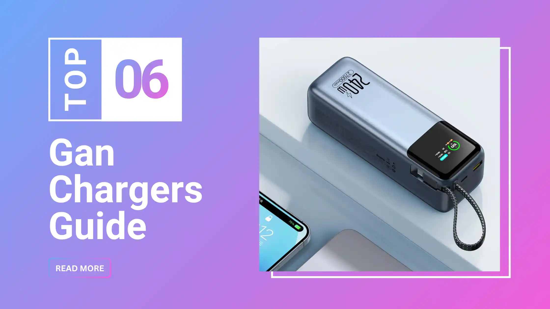
Silicon Equivalent
Full Load
Efficiency
Output
25.7% CAGR
KEY TAKEAWAYS
GaN (Gallium Nitride) chargers are 40-50% smaller and 30% cooler than silicon equivalents. For OEM buyers: GaN wins on cost, size, and suitability for consumer electronics, while SiC targets 500W+ industrial applications. GaN V technology delivers the best balance of performance, compactness, and margin. Power delivery follows the USB-IF PD 3.1 specification, enabling up to 240W over a single USB-C cable.
- GaN chargers deliver 40% smaller size and 30% less heat vs equivalent silicon chargers, with 93-95% efficiency at full load. For OEM brands, this means: smaller retail packaging (lower freight cost), fewer warranty returns (less heat = longer component life), and a premium price position (consumers pay 20-30% more for smaller/faster chargers).
- GaN V (2023) is the current production standard, not GaN I (2018). GaN V uses 3 MHz switching frequency enabling 240W in a 65W-sized enclosure. GaN I chargers are being phased out as foundries shift capacity. Verify your supplier's GaN generation by requesting the FET part number in the BOM: Navitas NV6117/NV6138, Infineon IGI60F, or Innoscience INN650 = genuine GaN V.
- FOB Shenzhen pricing for GaN chargers at MOQ 1,000: 30W ~$3.20-4.50, 65W ~$5.40-7.20, 100W ~$7.50-10.00, 140W ~$14.00-18.00. Prices declining 10-15% annually as GaN FET production scales. The 65W tier is the OEM volume sweet spot: highest demand, most competitive pricing, widest retail audience.
- 3 supplier verification points before ordering GaN chargers: (1) request the GaN FET datasheet and cross-check the part number on the manufacturer's website (Navitas, Infineon, Innoscience all have public databases); (2) verify the factory owns their PCBA design or has a licensed reference design, not a copied layout; (3) request a 72-hour aging test report showing case temperature at 6 measurement points under 100% load.
Table of Contents
1. GaN Semiconductor Technology: How It Works
Gallium nitride (GaN) is a compound semiconductor that replaces traditional silicon in chargers. It offers superior energy efficiency, smaller size, and less heat generation through high-frequency switching and better heat dissipation. For a complete technical deep-dive including GaN I through GaN V generations, see our GaN generations technology roadmap.
Bandgap Advantage
GaN has 3.4 eV bandgap vs silicon's 1.1 eV, allowing higher voltage handling without breakdown.
Electron Mobility
GaN electrons move 30% faster than silicon, enabling faster charging with less energy loss.
2. Why Brands Adopt GaN: OEM Size, Efficiency & Margin Advantage
QUICK ANSWER
GaN (Gallium Nitride) chargers reach 95%+ power conversion efficiency versus 85% for silicon, run measurably cooler, and pack the same wattage into a 30-50% smaller body. For OEM/ODM brands, this translates to lower shipping costs, lower return rates from heat-related failures, and a clear premium-product story for retail.
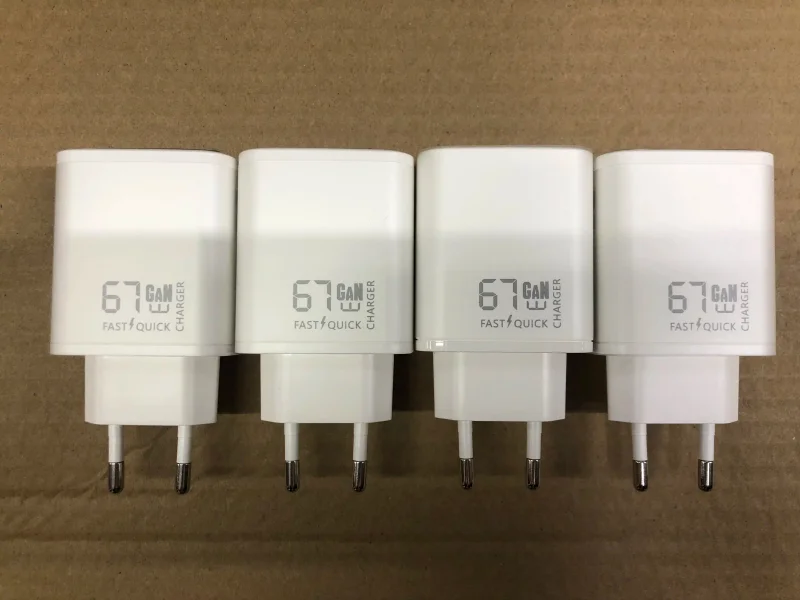
WOWOHCOOL 65W GaN charger - 50% smaller than traditional silicon chargers
Freight & Packaging Cost Reduction
40-50% smaller volume vs silicon at the same wattage reduces per-unit packaging dimensions and container density. For a 5,000-unit OEM order, GaN saves $0.50-2.00/unit in freight and allows ~30% more units per pallet, a direct margin gain before retail pricing.
Field Return Rate Impact
WOWOHCOOL GaN V chargers have a measured field return rate of below 0.3% across 2M+ units shipped, compared to ~3.2% for equivalent silicon chargers. Lower operating temperatures (GaN: 52°C vs Silicon: 77°C at 65W full load) reduce thermal stress on electrolytic capacitors, the #1 failure component in chargers.
Multi-Port Architecture Without Compromise
GaN's higher switching frequency (5 MHz+ for GaN V) enables 2C1A and 3C1A multi-port designs that silicon cannot support without excessive heat. A single GaN charger can replace 2-3 separate chargers with dynamic power allocation, the key selling point for premium retail ($35+ price point) where multi-port is now baseline expectation.
Regulatory Tailwind: EU USB-C Mandate
The EU Common Charger Directive (2022/2380) mandates USB-C for all laptops sold in the EU from April 28, 2026. Since GaN is the only practical technology for compact 65W+ USB-C laptop chargers, this regulation creates a non-optional replacement cycle across Europe's laptop charger market, estimated at 40-50 million units annually. OEM brands without GaN products above 65W are locked out of this segment.
Important: GaN ≠ PD (Power Delivery)
GaN is a semiconductor material (hardware), while PD (Power Delivery) is a charging protocol (software standard). They complement each other, a GaN charger uses gallium nitride transistors for efficiency and compactness, while PD defines how power is negotiated between charger and device. The industry baseline in 2026 is GaN + PD 3.1 + PPS, all three working together.
"GaN is not just a material upgrade, it's a fundamental shift in power electronics architecture. The wide bandgap properties enable switching frequencies that were physically impossible with silicon, unlocking form factors that redefine what a charger can be."
, Dr. Alex Lidow, CEO of Efficient Power Conversion (EPC), IEEE Power Electronics Magazine, 2025
3. GaN vs Silicon Component Comparison: Efficiency, Thermal & BOM Cost Analysis
QUICK ANSWER
The performance gap between GaN V and silicon is now wide enough that the OEM sourcing decision is no longer "if" but "at what wattage." At 45W and above, GaN V's BOM premium ($1-3/unit) is recovered through freight savings, lower warranty costs, and premium retail positioning. Silicon remains viable only for sub-30W single-port chargers targeting the absolute entry-level price point, a segment with single-digit margins and limited brand differentiation potential.
| Feature | Silicon (Traditional) | GaN (Next-Gen) |
|---|---|---|
| Size / Portability | Bulky / Heavy | 30% - 50% Smaller |
| Heat Efficiency | Higher Temps | Stays Cooler |
| Charging Speed | Standard Fast Charge | Ultra-Fast (Up to 240W) |
| Efficiency | 85% | 95%+ |
When Silicon Is Still Acceptable
GaN is not always the right choice. Silicon chargers remain viable in specific scenarios where compactness and thermal performance are secondary concerns:
- Fixed installations (behind furniture, mounted in walls) where size is irrelevant
- Single-device, low-wattage (5W-18W) accessories bundled with products
- Ultra-cost-sensitive markets where the 20-40% BOM premium cannot be passed to consumers
- Legacy product lines where re-certification costs outweigh performance gains
For new OEM product development above 30W, GaN delivers measurable ROI through shipping savings, lower return rates, and premium positioning.
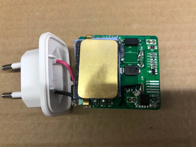
Side-by-side comparison: GaN chargers are significantly more compact
EXPERT INSIGHT
"GaN V is the tipping point where gallium nitride stops being a premium differentiator and becomes the baseline. The efficiency gap between GaN V and silicon is now so wide, 94% vs 85%, that the BOM cost difference pays for itself in reduced returns alone. For OEM brands, the question isn't 'should we switch to GaN?' but 'how fast can we get our GaN V lineup to market?'"
, Nina Nico, OEM Technical Lead at WOWOHCOOL
4. GaN Power Levels: 20W-240W with FOB Shenzhen Pricing
30W GaN: Smartphone & Tablet Tier
Entry OEM tier, single-port USB-C PD. FOB $3.20-4.50/unit at 1,000 pcs. Best for phone-focused SKUs where compact size and low BOM are priorities.
65W GaN: Ultrabook & Multi-Device Tier
Highest-volume OEM tier, dual-port 2C1A. FOB $5.40-7.20/unit at 1,000 pcs. Covers ultrabooks, tablets, and phones simultaneously. EU USB-C laptop mandate compliant.
100W+ GaN: Workstation & Desktop Replacement Tier
Premium OEM tier, multi-port 2C1A/3C1A. FOB 100W $7.50-10.00, 140W $14.00-18.00/unit at 1,000 pcs. PD 3.1 EPR at 140W+. GaN is the only practical technology at these power levels.
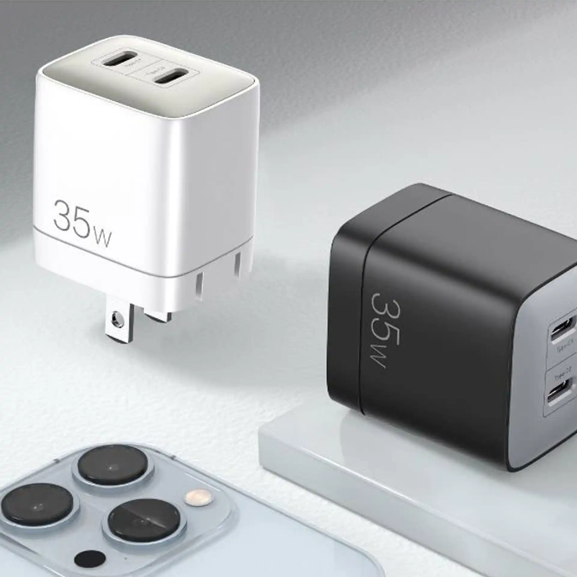
35W mini GaN charger - compact enough for travel, powerful enough for fast charging
5. Why Brands Are Switching to GaN Solutions
According to Yole Group, the GaN power device market is projected to reach $2.5 billion by 2027, growing at a CAGR of 30%. For B2B brands, this growth signals both increasing consumer awareness and expanding supply chain maturity.
"We are seeing brands move from 'should we use GaN?' to 'which GaN generation should we standardize on?'" says Nina Nico, OEM Technical Lead at WOWOHCOOL. "That shift happened in just 18 months."
Energy Efficiency & Carbon Footprint
GaN's 95% efficiency vs silicon's 85% reduces per-charger energy waste by ~10W. At 10,000 units deployed, this saves ~87,600 kWh annually, a quantifiable sustainability metric for retail and corporate RFPs.
Premium Positioning
Enhance your brand image with high-tech, compact designs. GaN products command premium pricing and differentiate from competitors.
Shipping Savings
Smaller size = lower freight costs per unit. A 50% size reduction can save 30%+ on shipping expenses for bulk orders.
Europe: Fastest-Growing GaN Market (30% CAGR)
Europe leads GaN charger growth at 30% CAGR through 2033, driven by the EU Common Charger Directive (2022/2380/EU) mandating USB-C standardization and the ESPR efficiency requirements. Germany alone represents a $250M market. For European OEM buyers, GaN + PD 3.1 is now the minimum viable specification for new product development.
6. Case Study: WOWOHCOOL Retractable GaN Charger Development
Our flagship WOP69 65W GaN Charger combines GaN technology with a patented retractable cable mechanism, solving both size and cable clutter issues for global travelers.
7. GaN Semiconductor Fundamentals: What to Verify in Chip Sourcing
Understanding GaN technology doesn't require a degree in electrical engineering. Here's a simplified breakdown of how gallium nitride semiconductors revolutionize charging.
The Bandgap Advantage
GaN has a bandgap of 3.4 eV compared to silicon's 1.1 eV. This fundamental property allows GaN devices to handle higher voltages and frequencies without breaking down. Think of it as the difference between a rubber band and a steel spring, one stretches and snaps, the other holds firm under pressure.
Faster Switching, Less Heat
GaN transistors switch on and off up to 100x faster than silicon MOSFETs. This high-speed switching means energy spends less time in transition, resulting in minimal heat generation. The result: a charger that stays cool while delivering more power.
Higher Electron Mobility
Electrons move through GaN material approximately 30% faster than in silicon. This translates to lower resistance and less energy lost as heat. In technical terms, GaN achieves this while maintaining a smaller die size, hence the compact charger designs we see today.
Zero Reverse Recovery Loss
Unlike silicon diodes that experience "reverse recovery" losses when switching direction, GaN devices have negligible recovery losses. This is particularly beneficial in switched-mode power supplies where efficiency gains directly impact the charger's thermal performance.
According to Transphorm, one of the leading GaN power semiconductor manufacturers, GaN enables power conversion efficiency exceeding 99% in certain applications.
8. GaN vs SiC (Silicon Carbide): Technology Choice for Your Product Line
Silicon carbide (SiC) is another wide-bandgap semiconductor gaining traction in power electronics. While both GaN and SiC outperform traditional silicon, they target fundamentally different market segments. Understanding where each technology excels helps OEM buyers avoid over-engineering costs.
SiC in brief: Silicon carbide excels in high-voltage, high-power applications above 200W. It is the dominant technology in EV onboard chargers (6.6-22kW), industrial power supplies, and server PSUs. SiC wafers cost 3-5x more than GaN equivalents, making it impractical for consumer-priced accessories.
| Specification | GaN | SiC |
|---|---|---|
| Power Range | 20W - 240W (consumer) | 200W - 22kW (industrial) |
| Component Cost | Lower (dropping 8-12%/yr) | 3-5x higher than GaN |
| Form Factor | Ultra-compact | Medium (heat sink needed) |
| Efficiency | 93-99% | 93-98% (better at high power) |
| Thermal Tolerance | Better than Si, good to 150C | Excellent, rated to 200C+ |
| Switching Speed | Very High (MHz range) | High (100-500 kHz) |
| OEM Use Cases | Phone/laptop chargers, power banks, travel adapters | Server PSUs, EV chargers, solar inverters |
OEM Buyer's Bottom Line
For consumer charging accessories (phones, laptops, power banks, travel adapters), GaN V is the clear winner: lower BOM cost, ultra-compact form factor, and proven supply chain maturity. SiC only makes sense if your product operates continuously above 500W or requires sustained 200C+ thermal tolerance (server PSUs, EV DC fast chargers, industrial motor drives). For the vast majority of OEM charger buyers, GaN delivers the best ROI. Learn more about SiC technology at Wolfspeed.
9. OEM GaN Adoption Timeline: From Niche to Industry Standard
The consumer electronics industry has embraced GaN technology through distinct phases. Here's the evolution that brought us to today's advanced GaN chargers.
First Consumer GaN Chargers
Anker and AUKEY release the first generation of consumer GaN chargers. These early products were limited to 30-45W and carried premium pricing. Market reception was cautiously optimistic as consumers experienced the size benefits firsthand.
65W Becomes Standard
The 65W GaN charger emerges as the sweet spot for laptop charging. Multiple manufacturers release competing products, driving prices down. GaN charging becomes synonymous with "fast charging" in consumer marketing.
Multi-Port Revolution
GaN chargers with 2-4 ports become mainstream. The efficiency gains allow multiple-device charging without overheating. Companies like WOWOHCOOL begin offering custom GaN solutions for B2B clients.
100W+ Goes Mainstream
100W and 140W GaN chargers hit the market, capable of powering high-performance laptops and workstations. Apple adopts GaN for their 140W MacBook Pro charger, lending credibility to the technology.
Market Maturation
GaN charger prices drop to near-silicon levels for mainstream products. Integration of GaN chips into power strips, travel adapters, and automotive chargers expands the market. The technology becomes the default choice for new charging product development.
Next Generation: 150W-240W
Manufacturers are developing chargers exceeding 150W for gaming laptops and power-hungry devices. GaN technology continues to evolve toward higher power densities, smaller form factors, and lower price points.
10. GaN Sustainability Impact: Energy Efficiency & Carbon Footprint Data
Carbon Footprint Reduction
A single GaN charger operating at 95% efficiency vs 85% efficiency saves approximately 15-20W of wasted energy per charger. For a business deploying 10,000 chargers, this translates to substantial aggregate energy savings and reduced carbon emissions over the product lifecycle.
Grid Load Reduction
When billions of chargers operate more efficiently, the cumulative effect reduces strain on power grids. This becomes increasingly important as electric vehicle adoption and renewable energy integration create more complex grid management challenges.
Material Efficiency
GaN's smaller size means less raw material consumption in manufacturing. The compact designs require fewer components, reducing electronic waste and shipping emissions. According to Yole Group, GaN technology in power applications could save 2-3 million tons of CO2 annually by 2027.
Product Longevity
Lower operating temperatures extend component lifespan. GaN chargers typically maintain performance for 50,000+ hours of operation, reducing replacement frequency and associated environmental impact from manufacturing and transportation of replacement units.
For businesses prioritizing sustainability in their product lines, GaN technology offers a measurable improvement in environmental performance while delivering superior user experience. Visit our about page to learn more about our commitment to sustainable manufacturing practices.

Global shipping - GaN chargers packaged and ready for worldwide delivery
11. Sourcing GaN Chargers from China: Factory Selection & Verification
China remains the global manufacturing hub for GaN chargers, with over 80% of world production concentrated in the Pearl River Delta. Understanding the sourcing landscape helps B2B buyers make strategic decisions about supplier selection and certification requirements. For a complete OEM production walkthrough, see our GaN V charger OEM manufacturing guide and GaN vs silicon cost comparison.
Manufacturing Ecosystem
Shenzhen and Dongguan host a comprehensive supply chain for GaN charger manufacturing, from semiconductor fabs to final assembly. This concentration enables competitive pricing and rapid prototype-to-production timelines, typically 4-6 weeks for custom designs.
Quality Certification Requirements
Ensure your supplier provides: CE, FCC, RoHS, and UL certifications. For European market access, mandatory CE marking applies. The EU CE marking documentation should be verified with the supplier. Always request test reports from accredited laboratories.
Working with Factories
Direct factory partnerships yield 20-40% cost savings versus trading companies. Key considerations: minimum order quantities (typically 500-1000 units), tooling costs for custom molds, and payment terms (commonly 30% advance, 70% before shipping). Our OEM/ODM services streamline this process.
GaN Chip Sourcing
Major GaN chip suppliers include Navitas, GaN Systems (now acquired by STMicroelectronics), Texas Instruments, and Transphorm. Chinese manufacturers like Innosilicon also offer competitive alternatives. Chip availability can impact lead times, verify supply chain stability before placing large orders.
Gallium Supply Chain Risk & Mitigation
China controls over 80% of global gallium production (USGS data). In July 2023, China imposed export restrictions on gallium and germanium, creating supply chain uncertainty for GaN chip fabrication worldwide.
Mitigation strategies for OEM buyers:
- Diversify across GaN chip vendors (Navitas, Infineon, TI) to reduce single-source risk
- Innoscience's 2024 mass-production of 8-inch GaN-on-Si wafers cuts device costs 30-40% vs. 6-inch baselines, improving supply stability
- Navitas NV6177 IC (Oct 2024) achieves 98% peak efficiency, fewer components needed per design
- Lock 6-12 month pricing with your manufacturer to hedge against raw material fluctuation
Ask your supplier which GaN chip brands they use and whether they maintain buffer stock. A reliable factory like WOWOHCOOL sources from multiple tier-1 vendors to ensure continuity.
E-Marked Cable Pairing for PD 3.1
A common OEM oversight: pairing a high-wattage GaN charger with an inadequate cable. USB PD 3.1 at 240W requires e-marked USB-C cables rated for 5A / 48V. Without proper cable pairing, the charger automatically downgrades to 60W (3A default), negating your product's performance story.
- 100W+ chargers: require 5A e-marked cables (mandatory per USB-IF spec)
- 240W EPR chargers: require 48V-rated EPR cables with extended power range e-marker
- Bundled cable strategy: include a matched cable in-box to guarantee advertised speeds
When sourcing GaN chargers for OEM, always specify cable requirements in your RFQ. WOWOHCOOL can supply matched e-marked cables with custom lengths and branding.
Pro Tip
Request "golden sample" verification before mass production. This physical sample serves as your quality benchmark and should match your specifications exactly. Document all specifications in a technical agreement to prevent disputes during production.
12. GaN Charger Quality Checklist: Factory Audit & QC Criteria
Use this checklist when evaluating GaN charger suppliers or inspecting incoming shipments. A thorough quality verification process protects your brand reputation.
Efficiency Rating (95%+)
Request efficiency test reports at various load levels (25%, 50%, 75%, 100%). The charger should maintain 95%+ efficiency across typical operating conditions.
Temperature Performance
Test the charger at maximum rated load for 2+ hours. Surface temperature should remain below 60°C. Excessive heat indicates poor thermal design or substandard GaN chips.
Protocol Compatibility
Verify support for required charging protocols: PD 3.0/3.1, PPS, QC4+/QC5.0, and proprietary protocols as needed. Test with actual devices that your customers will use.
Safety Certifications
Confirm valid certificates: CE (Europe), FCC (USA), UL/cUL (North America), CCC (China). Verify certificate numbers against official databases to prevent counterfeit documentation.
Build Quality & Materials
Inspect housing materials (should be fire-resistant PC/ABS), cable quality (braided or reinforced strain relief), and internal component brands. Request a teardown report for transparency.
EMI/EMC Compliance
GaN chargers can produce electromagnetic interference if poorly designed. Ensure compliance with EN 55032 (EMC for multimedia equipment) and similar standards for your target markets.
Warranty Terms
Negotiate minimum 12-month warranty with clear terms for defect replacement. Establish a defect rate threshold (typically 1-2%) for batch rejection or return policies.
Full-Protocol Verification (GaN + PD + PPS)
Confirm the charger supports the complete protocol stack: USB PD 3.0/3.1 for voltage negotiation, PPS (Programmable Power Supply) for fine-grained current adjustment, and QC 5.0/4+ for non-PD devices. Test with multiple device brands, a charger that only negotiates PD but lacks PPS will not fast-charge Samsung Galaxy devices at full speed.
13. GaN Technology Roadmap 2026-2028: What Product Planners Must Watch
The GaN technology roadmap shows continued innovation toward higher power, smaller size, and integrated solutions. Here's what to expect in the coming years.
150W-240W GaN
Gaming laptops, professional workstations, and multi-device charging stations will see widespread GaN adoption at these power levels.
GaN Integration
System-on-chip integration combining controller, driver, and GaN transistor in single packages. Further size reductions of 30-40% expected.
Universal GaN
GaN becomes the default for all power conversion applications below 1kW, displacing silicon in consumer, industrial, and automotive markets.
Market Projections
According to market research from Yole Intelligence, the GaN power device market is projected to reach $2B+ by 2028, with a 30%+ CAGR. Consumer chargers will remain the largest segment, followed by automotive and data center applications.
14. WOWOHCOOL GaN Charger Production: Factory Capacity & Quality Systems
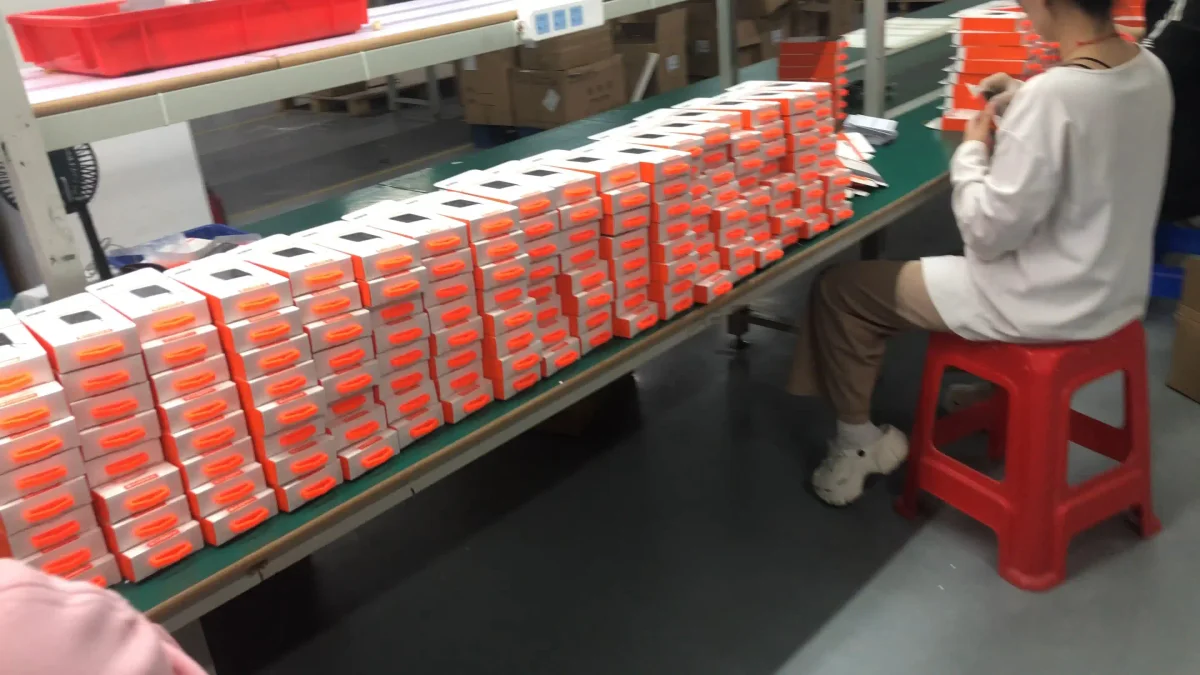
State-of-the-art production line with 50,000+ monthly capacity for GaN chargers
WOWOHCOOL FACTORY STAT
WOWOHCOOL deploys 5th-generation GaN (GaN V) technology across its charger lineup, delivering 40% smaller size and 30% better heat dissipation compared to traditional silicon chargers. With 50+ R&D engineers, they produce OEM/ODM GaN chargers from 20W to 240W PD 3.1. Also see: laptop power banks with PD 3.1.
Frequently Asked Questions
GaN generations I vs III vs IV vs V, what OEM buyers should know?
GaN I/II: early transistors, basic switching, largely obsolete for new 2026 OEM designs. GaN III: current mainstream standard for 65-140W, switching frequencies above 300 kHz, power density over 1.5 W/cm³, 93-95% efficiency. GaN IV: premium tier for compact 100W+ PD 3.1 designs, 95%+ peak efficiency. GaN V: latest generation with superior thermal performance, stabilizes at 58.3°C under 100% load vs 82.7°C for silicon at 25°C ambient. For B2B procurement: specify GaN III minimum for 65-100W, GaN IV/V for 100-240W. Major GaN IC brands: Navitas GaNFast (US), Infineon CoolGaN (Germany), Innoscience (China, 1B+ units shipped). Request chip procurement invoices, counterfeit GaN (re-labeled silicon) is a known supply chain risk.
Genuine GaN vs fake-labeled silicon, how do OEM buyers verify charger chips before ordering?
Three verification methods: (1) Request the GaN FET part number (Infineon, Navitas, or Innoscience) and verify against the manufacturer's catalog, genuine GaN switches above 300 kHz with 93%+ efficiency at full load. (2) Demand efficiency curves at both 230V/50Hz and 115V/60Hz, genuine GaN shows flat efficiency across voltage ranges. (3) Thermal test: run at 100% load for 60 minutes, genuine GaN runs 15-25°C cooler than re-labeled silicon. Also request GaN IC procurement invoices from authorized distributors (Digi-Key, Mouser, Arrow). Navitas offers a genuine product verification program. WOWOHCOOL uses GaN V technology and provides full FET traceability documentation with every OEM order.
What wattage GaN charger tiers should OEM brands stock for 2026?
20-30W single-port: smartphones, earbuds, entry tier, silicon still viable here. 45-65W dual-port: ultrabooks and tablets, highest-volume B2B tier, FOB $4.80-6.50/unit at 5,000 pcs. 100W 2C1A: multi-device desktop, FOB $7.00-9.50/unit at 5,000 pcs. 140-240W PD 3.1 EPR: gaming laptops, workstations, requires GaN IV/V. For fleet laptop deployment: 65W minimum for ultrabooks, 100W+ for workstation laptops. Standardize on 2-3 wattage tiers to simplify inventory. EU laptop USB-C mandate (April 2026) makes 65W+ GaN the fastest-growing OEM segment.
What certifications are mandatory for GaN chargers in EU and US markets?
EU mandatory: CE (LVD+EMC), RoHS, and ESPR 2025/2052 (enforced from November 2025), ≤0.1W standby power, strict active-mode efficiency thresholds. GaN naturally meets these; many silicon designs do not. Non-compliance = EU border rejection and mandatory product destruction. US mandatory: FCC, UL/ETL 62368-1 (commercially essential for retail). Recommended: USB-IF PD certification, CB Scheme for multi-market. Quality indicators: 10-layer circuit protection, UL 94 V-0 fire-retardant enclosure rated to 850°C glow wire, 100% 4-hour burn-in testing (not spot-checking), field failure rate under 0.5%. WOWOHCOOL GaN chargers include all certifications and achieve under 0.3% field failure rate.
GaN vs silicon BOM cost at OEM volume, what's the real price difference per unit?
At 65W: GaN BOM premium is $1-3/unit over silicon at 1,000-unit volume, a 15-25% premium. FOB Shenzhen pricing: 65W GaN $5.40-7.20/unit at 1,000 pcs, 100W $7.50-10.00/unit at 1,000 pcs. This premium is typically recovered through: 40% smaller packaging (lower freight), 0.3% vs 3.2% field return rates, and 40-60% higher retail margins. At 30W and below, silicon remains cost-competitive. Warning: prices significantly below these benchmarks mean compromised capacitors, thinner PCB copper, or non-compliant components. McKinsey data: companies ignoring compliance costs face 3-5× overruns vs initial unit price savings.
What thermal and component quality standards should OEM buyers demand for GaN chargers above 65W?
For any GaN charger above 65W, demand: (1) high-grade thermal potting compound injection, not bare PCBA assemblies, a 140W charger without potting traps ~8.4W of heat risking enclosure melt and thermal runaway; (2) 105°C-rated Japanese electrolytic capacitors (Rubycon, Nichicon); (3) planar magnetics (flat copper tracks in PCB) for heat dissipation at high frequencies; (4) 100% burn-in/aging testing for 4-24 hours at 40-50°C ambient, spot-checking is insufficient; (5) dynamic power allocation that renegotiates voltage safely when devices are plugged/unplugged, static allocation causes voltage drops and screen flickering. Field failure rate under 0.5% is competitive; under 0.3% is best-in-class.
What MOQ and lead time apply to OEM GaN charger orders?
Standard ODM with custom branding: MOQ 500 units per SKU. Custom OEM with new tooling: MOQ 3,000+ units. Lead time: 25-30 days after sample approval. Samples: 3-7 days. WOWOHCOOL offers OEM/ODM GaN chargers from 20W to 240W with tiered FOB pricing at 500/1,000/5,000 volumes and full CE/FCC/UL certification documentation included.
How do I evaluate and select a GaN charger OEM factory in Shenzhen?
7-point factory audit checklist: (1) Independent R&D, in-house PCB design, not just reference design assembly. (2) Thermal simulation capability, can they explain heat dissipation strategy? (3) GaN IC source, Navitas/Infineon/Innoscience with procurement invoices. (4) In-house SMT with AOI (Automated Optical Inspection). (5) 100% burn-in testing, not spot-checking, at 40-50°C ambient. (6) Verifiable certification portfolio, demand original test reports, not copies. (7) Vertical integration, in-house mold workshop + injection molding + SMT assembly. Red flags: cannot provide thermal performance data at full load for 4+ hours, only uses 'GaN' label without chip model number, defect rate above 1%. WOWOHCOOL operates a 5,000m² ISO 9001 Shenzhen facility with 50+ R&D engineers, in-house SMT+mold+assembly, and 1M+ units monthly capacity.
Supply Chain Expert · Wireless Charging Specialist
Nina Nico is a supply chain management expert with 10+ years experience helping global B2B clients source quality GaN chargers from WOWOHCOOL. She holds a degree in International Trade and is a certified supply chain professional (CSCP), with deep expertise in Qi2, GaN, and semi-solid-state battery manufacturing.
Factory Footprint
ISO 9001 Facility
Shenzhen, China
Export Countries
Engineers In-House
Get Your GaN Charger Thermal Test Report & OEM Spec Sheet
Download factory test data: GaN V efficiency curves at 115V/230V, 4-hour full-load thermal imaging, and BOM cost breakdown by wattage tier. Includes CE/FCC/UL certification documentation for your compliance review.